- 您现在的位置:买卖IC网 > Sheet目录320 > DK-DEV-4SGX530N (Altera)KIT DEVELOPMENT STRATIX IV
�� �
�
�6–4�
�Chapter� 6:� Board� Test� System�
�Using� the� Board� Test� System�
�Using� the� Board� Test� System�
�This� section� describes� each� control� in� the� Board� Test� System� application.�
�The� Configure� Menu�
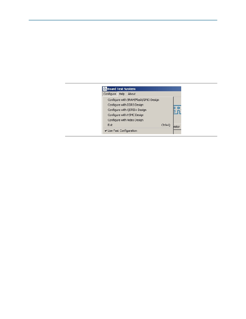
�Use� the� Configure� menu� (� Figure� 6–2� )� to� select� the� design� you� want� to� use.� Each� design�
�example� tests� different� board� features.� Choose� a� design� from� this� menu� and� the�
�corresponding� tabs� become� active� for� testing.�
�Figure� 6–2.� The� Configure� Menu�
�To� configure� the� FPGA� with� a� test� system� design,� perform� the� following� steps:�
�1.� On� the� Configure� menu,� click� one� of� the� following� options� to� determine� how� to�
�pass� data� through� the� JTAG� chain:�
�■�
�■�
�Use� Fast� Configuration� —Compresses� the� data� for� faster� loading.�
�Use� Quartus� II� Programmer� —Uses� the� standard� JTAG-based� configuration�
�method.�
�2.� On� the� Configure� menu,� click� the� configure� command� that� corresponds� to� the�
�functionality� you� wish� to� test.�
�3.� In� the� dialog� box� that� appears,� click� Configure� or� Download� Start� to� download�
�the� corresponding� design’s� SRAM� Object� File� (� .sof� )� to� the� FPGA.� The� download�
�process� usually� takes� about� a� minute.�
�4.� When� configuration� finishes,� close� the� Quartus� II� Programmer,� if� using� it.� The�
�design� begins� running� in� the� FPGA.� The� corresponding� GUI� application� tabs� that�
�interface� with� the� design� enable.�
�The� Config� Tab�
�The� Config� tab� shows� information� about� the� board’s� current� configuration.�
��MAX� II� registers,� the� JTAG� chain,� the� board’s� MAC� address,� the� flash� memory� map,�
�and� other� details� stored� on� the� board.�
�The� following� sections� describe� the� controls� on� the� Config� tab.�
�Board� Information�
�The� Board� information� controls� display� static� information� about� your� board.�
�Stratix� IV� GX� FPGA� Development� Kit� User� Guide�
�March� 2014� Altera� Corporation�
�发布紧急采购,3分钟左右您将得到回复。
相关PDF资料
DK-DEV-5AGXB3N/ES
ARRIA V DEVELOPMENT KIT
DK-DEV-5M570ZN
KIT DEV MAX V 5M570Z
DK-DEV-5SGXEA7N
KIT DEV STRATIX V FPGA 5SGXEA7
DK-DSP-2S180N
DSP PRO KIT W/SII EP2S180N
DK-DSP-3C120N
KIT DEV DSP CYCLONE III EDITION
DK-K7-CONN-CES-G
KINTEX-7 FPGA CONNECTIVITY KIT
DK-K7-EMBD-CES-G-J
KINTEX-7 FPGA EMBEDDED KIT JAPAN
DK-MAXII-1270N
KIT DEV MAXII W/EPM 1270N
相关代理商/技术参数
DK-DEV-5AGTD7N
功能描述:可编程逻辑 IC 开发工具 FPGA Development Kit For 5AGTD7K3F40I3N
RoHS:否 制造商:Altera Corporation 产品:Development Kits 类型:FPGA 工具用于评估:5CEFA7F3 接口类型: 工作电源电压:
DK-DEV-5AGXB3N/ES
功能描述:可编程逻辑 IC 开发工具 FPGA Development Kit For 5AGXFB3H6F ES RoHS:否 制造商:Altera Corporation 产品:Development Kits 类型:FPGA 工具用于评估:5CEFA7F3 接口类型: 工作电源电压:
DK-DEV-5ASTD5N
功能描述:KIT DEV ARRIA V FPGA 制造商:altera 系列:Arria V ST 零件状态:在售 类型:FPGA 配套使用产品/相关产品:Arria? V ST 内容:板 标准包装:1
DK-DEV-5CEA7N
功能描述:可编程逻辑 IC 开发工具 FPGA Development Kit For 5CEFA7F31C7N
RoHS:否 制造商:Altera Corporation 产品:Development Kits 类型:FPGA 工具用于评估:5CEFA7F3 接口类型: 工作电源电压:
DK-DEV-5CEA7N/P
制造商:Altera Corporation 功能描述:Cyclone VE Devkit Promotional 制造商:Altera 功能描述:Cyclone VE Devkit Promotional
DK-DEV-5CEA7NES
功能描述:可编程逻辑 IC 开发工具 FPGA Development Kit For 5CEFA7F3
RoHS:否 制造商:Altera Corporation 产品:Development Kits 类型:FPGA 工具用于评估:5CEFA7F3 接口类型: 工作电源电压:
DK-DEV-5CEA7NESP
制造商:Altera Corporation 功能描述:KIT DEVELOPMENT CYCLONE V E
DK-DEV-5CEA7NP
制造商:Altera Corporation 功能描述:Cyclone VE Devkit Promotional 制造商:Altera 功能描述:Cyclone VE Devkit Promotional